Getting an IMU up and running was the most challenging portion of the project, mostly due to poor hardware design on my
part. The total IMU death toll was 3; one of which was definitely burned out from exposure to > 3.3V and two of which
that probably were burned out but also may just not have worked (Turns out “absolute max voltages” in the electrical
characteristic sections of datasheets are more than just suggestions).
Saleae Logic 4 in action
The two theories I have about what caused my “hardware heartache” are:
Poor hardware implementation: the female headers I used to mount the IMUs had some connectivity issues in the soldering
and didn’t transmit the IMU responses from read/write communication attempts via SPI.
MSSP Issues: The PIC18F2553 has a built in MSSP that controls the SCK/MISO/MOSI lines for SPI communication. The MSSP
module has several documented issues detailed in the errata released by Microchip and the Microchip forums.
All in all, the fourth IMU ended up being the charm and I implemented a “bit banged” SPI emulation to overcome the potential
hardware issues with the PIC18F2553. This section of my Tipsy’s write up will focus on what eventually worked, as
well as some of the “gotchas” I had to figure out.
Debugging
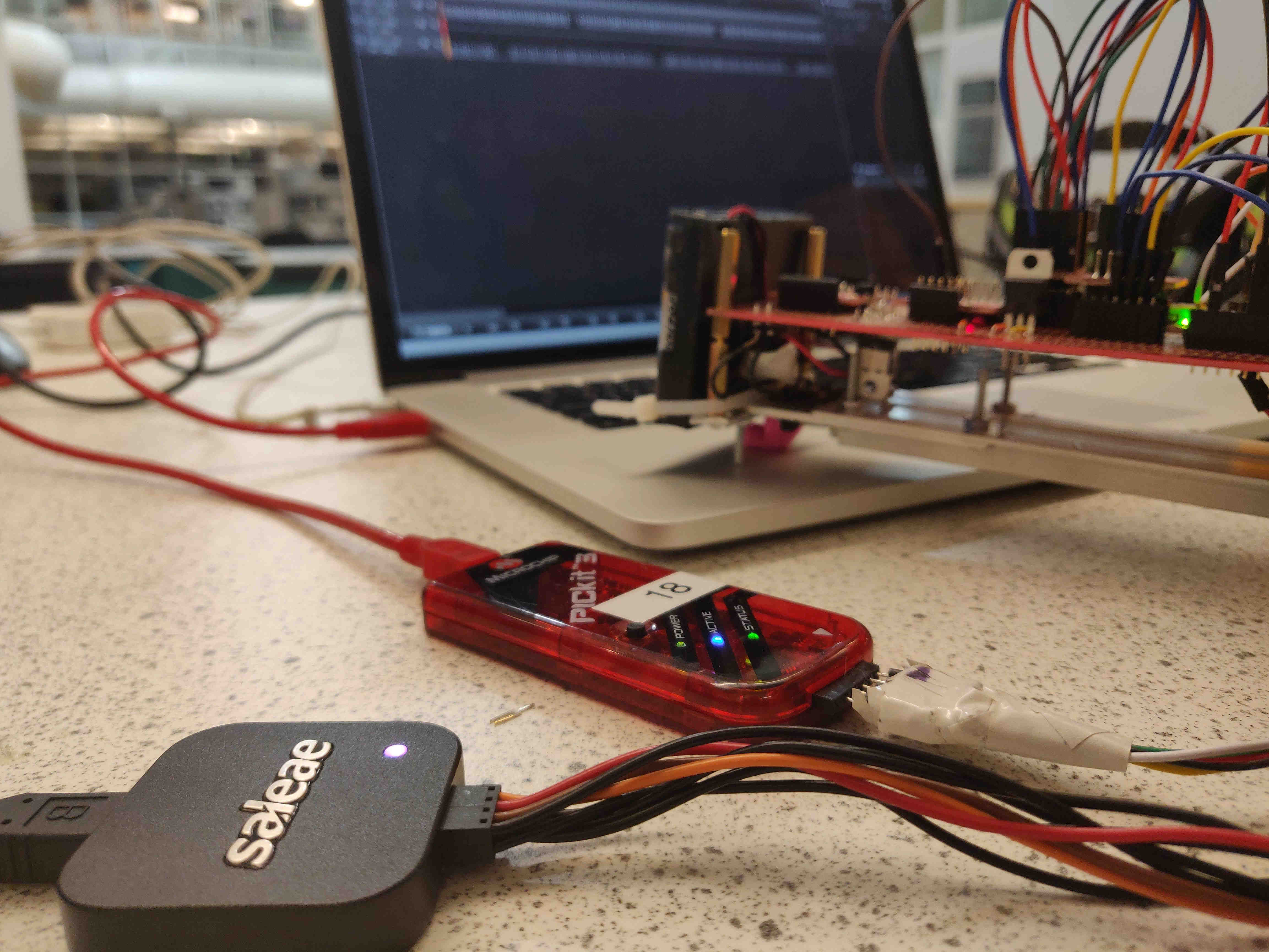
The two main debugging tools that I used during the IMU debacle were the PICkit3 In-Circuit Debugger (ICD) from
Microchip and the Saleae Logic 4 Logic Analyzer.
The Saleae Logic 4 was used to analyze the logic levels being output by the PIC, motor driver, and IMU in various scenarios
and was invaluable in the debugging process.
The PICkit3 was used to program the PIC18F2553 and access in-circuit
debugging functionality so I could add breakpoints/watches to my embedded code in realtime. The one major “gotcha” that
took some figuring out was how to enable ICD functionality on the PIC18F2553; the user code needs to manually enable ICD
functionality by setting the correct config bits:
1
2
#pragma config WDT=OFF        // clear this to turn off watchdog timer
#pragma config LVP=OFF        // clear this, allows debug to occur
These pragma statements are disabling the watchdog timer and disabling the single-side ICSP bit in the CONFIG2H and
not required and the ICD functionality worked by default.
### SPI Communication
I ended up trying 3 different IMU's on Tipsy:
1. ICM-20948 (x2, abandoned in place)
2. LSM6DS3
3. LSM9DS1
I eventually settled on the LSM9DS1, however all of the IMU's had similar communication schemas with some variation in
the register layout. Based on their respective data sheets, communication with the IMU's occurs in 16-bit operations
(occasionally more for multiple byte commands). The first byte transmitted is the address byte: the user sends the IMU
the address they'd like to read or write to. The most significant bit (MSB) of the address transmit dictates if the operation
is a "read" (MSB = 1) or "write" (MSB = 0) operation. The second byte transmitted is the command byte: in my experience
this is generally used to configure the address being written to. For read operations this can just be "dummy data" (I
typically just transmitted 0x00, however in theory it could probably be anything). Refer to the SPI communication waveforms
below from the Logic software for what a typical operation looks like:
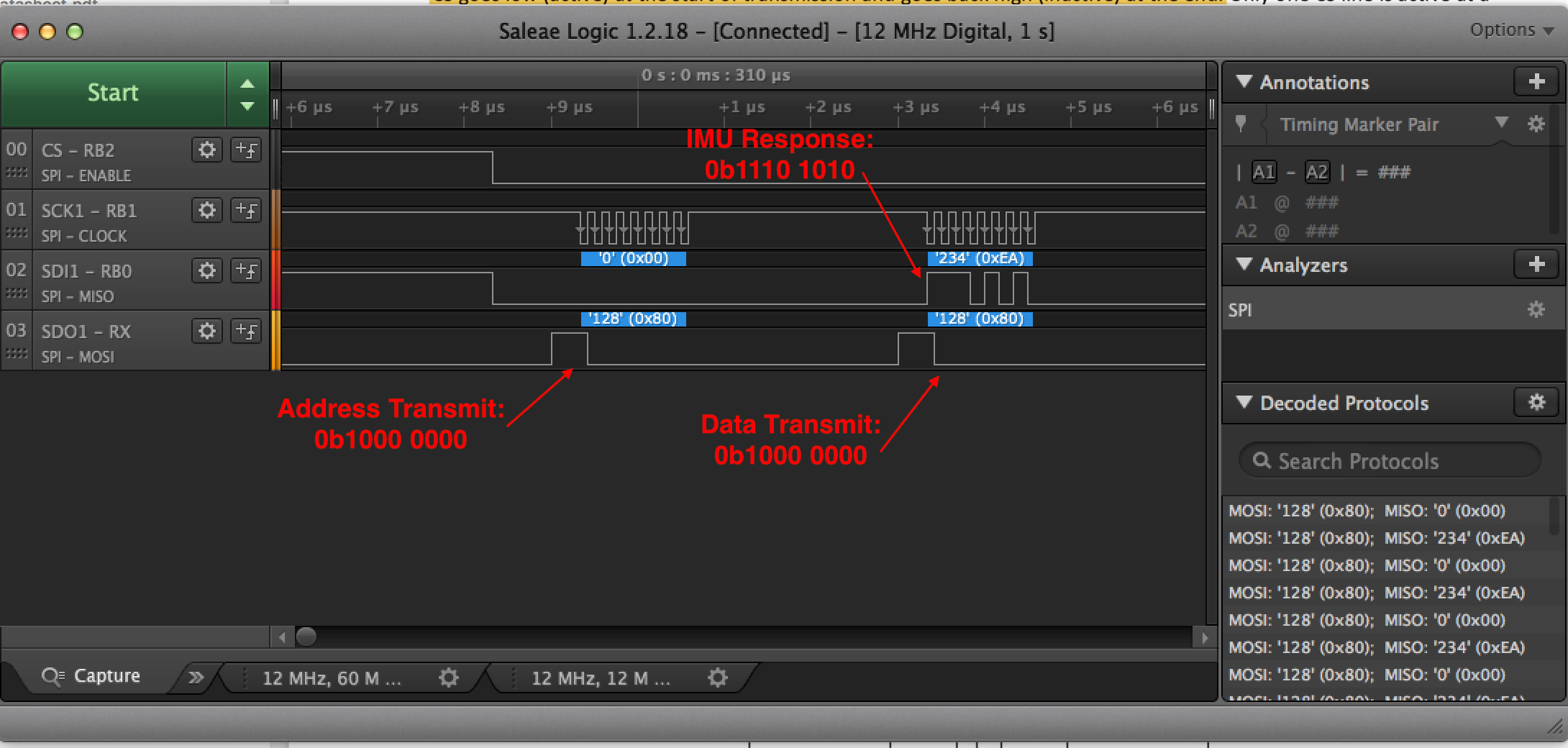
Typical SPI waveform
The waveform above was communicating with the ICM-20948. Based on the ICM-20948 data sheet, the ```WHO_AM_I``` address is
0x00and the expected response is0xEA. As seen in the SPI communication above, we set the address to0x00
and set the MSB = 1 for a read operation, resulting in a total communication byte of0x80. On the second byte transmission
we send dummy data (in this case we just resend0x80but technically anything should be fine) and the IMU responds with
its "ID code"0xEA``` which is the expected behavior per the ICM-20948 data sheet.
Although the IMU was able to respond with its name, I spent several long and frustrating hours trying to get any other sort
of response but was unsuccessful. I suspect this is due to a faulty MSSP module. I then switched to the LSM6DS3 which I
confirmed via Arduino was behaving properly:
Working chip prior to bad wiring
After patting myself on the back for figuring it out, I promptly burned it out due to faulty logic level converter wiring.
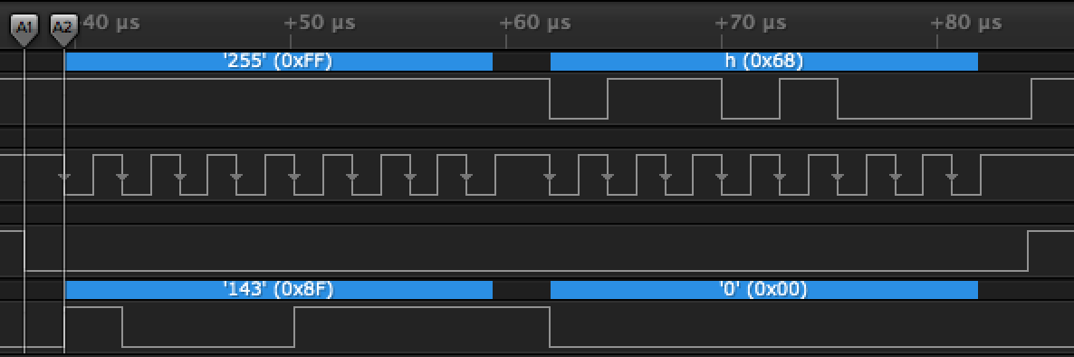
After some quick and dirty Dremel action to fix the wiring issue, I was able to get successful responses from the LSM9DS1. The WHO_AM_I register for
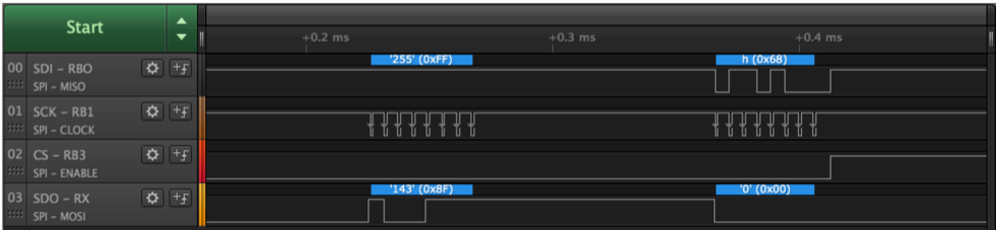
the LSM9DS1 is 0x0F and for a read operation the MSB = 1. As shown below it correctly responds with its ID code 0x68.
third fourth time is the charm
However, this value was not showing up on the PIC18F2553 when I put a watch using the ICD. I think that this was due to
poor soldering connections, however I did not fully troubleshoot due to time constraints.
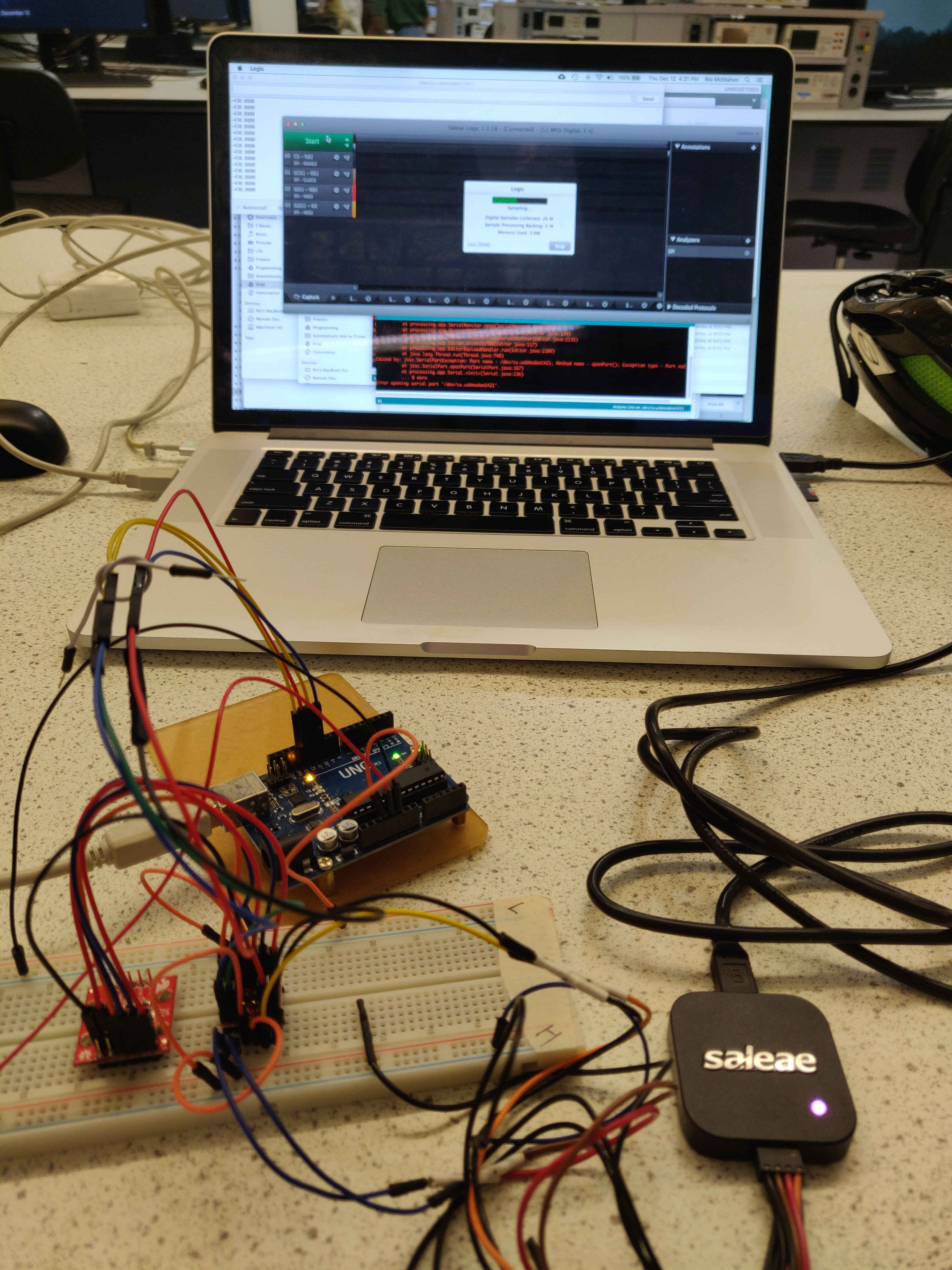
At this point I eventually used a software implementation of the SPI protocol rather than continuing to chase my tail with the
hardware/MSSP issues. This actually ended up being really simple using the Logic 4 and the Logic software; I just emulated
the SPI waveforms with software by toggling the appropriate pins to emulate the SCK, MOSI, and MISO 1 behavior that is
normally conducted by the MSSP. As shown in the output below, the SCK waveform is fairly janky but because the rising
edge and falling edge of the SCK is lined up with the MOSI bits, the logic analyzer and the IMU are able to successfully interpret them
and the IMU sends the expected response on the MISO line. We notice that we again receive the expected ID code from the
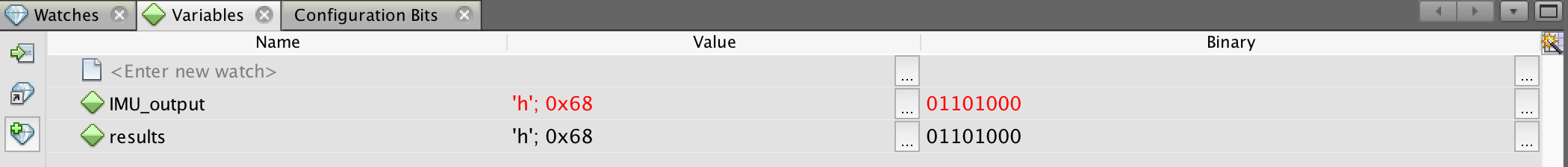
LSM9DS1, however this time we can also see it on the PIC18F2553 ICD watch.
Bit-Banged WHO_AM_I response from LSM9DS1
This was VERY exciting to see
After successfully being able to see the IMU output within the ICD watch configuring the IMU and reading from the
accelerometer/gyroscope was a comparative breeze.
At the end of the day, this was a very frustrating but also very educational experience. I chased my tail a lot going down
some forum rabbit holes when in reality it was probably just a bad solder connection. I recommend the Saleae Logic
analyzers/software for debugging because this phase of the project would have been substantially more painful without a
direct look at the SPI communication attempts from the PIC and the IMU(s). Their hardware design is clean and intuitive
to use and the functionality provided by their software is easy to interpret and debug with. I am looking forward to using
their line of logic analyzers during future embedded projects.
IMU #3 after meeting its fate
A quick note regarding terminology:MISO = Master In Slave Out (SDO line on LSM9DS1)MOSI = Master Out Slave In (SDA Line on LSM9DS1)SCL = Serial ClockCS = Chip Select (sometimes called SS for Slave Select)Read more about SPI here[return]